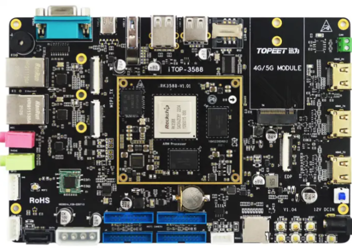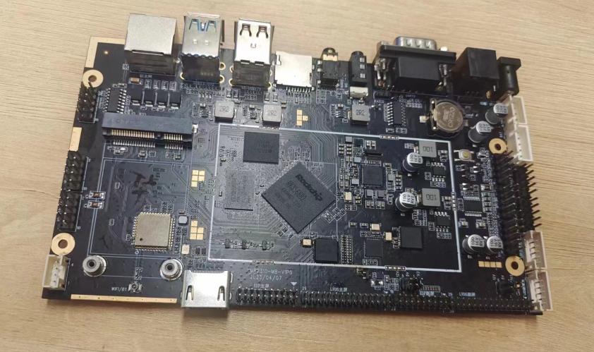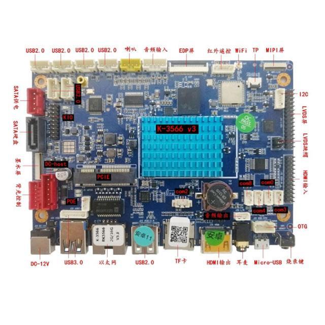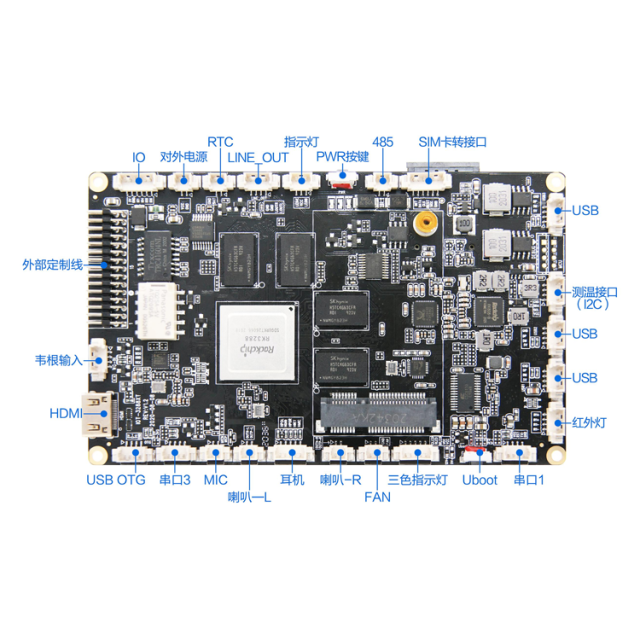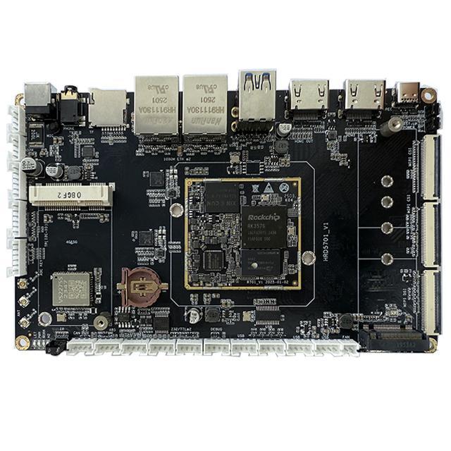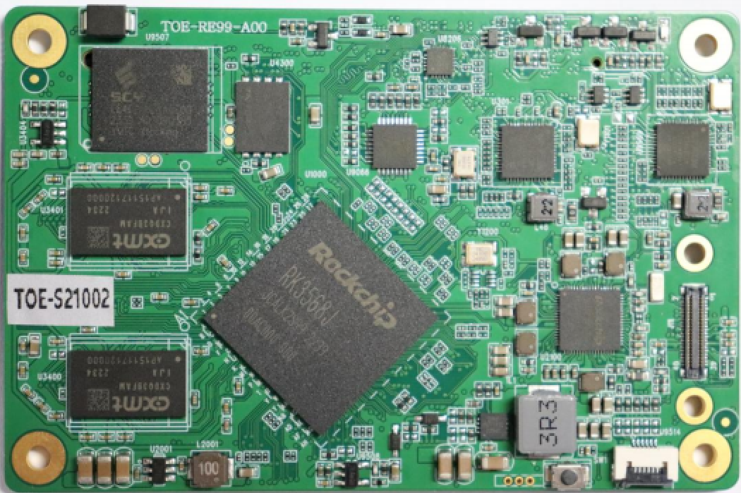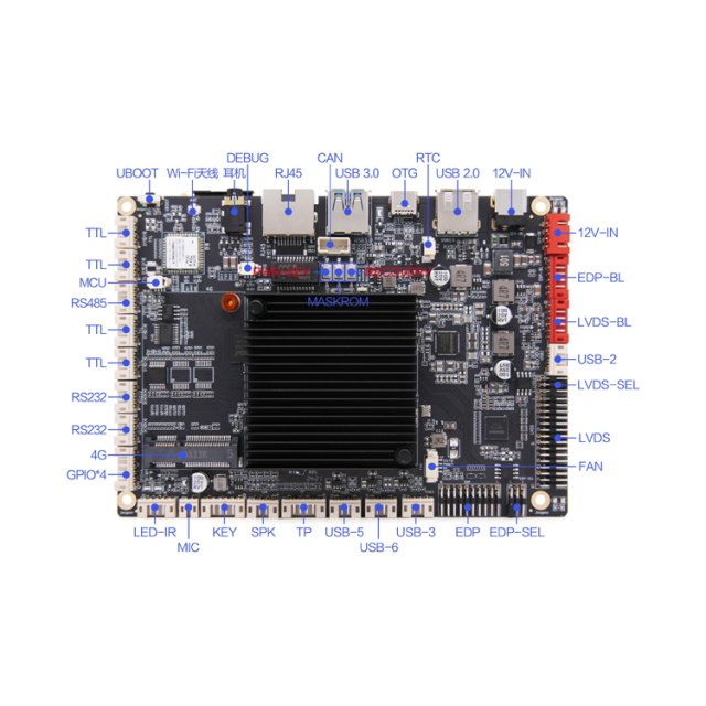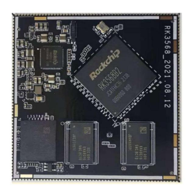
The RK3588 is Rockchip’s flagship 8nm ARM SoC, featuring four Cortex-A76 cores and four Cortex-A55 cores, an integrated 6 TOPS NPU, Mali-G610 GPU, multiple MIPI CSI/DSI interfaces, HDMI 2.1, PCIe 3.0, and USB 3.0. It is currently one of the mainstream high-performance platforms for edge AI, industrial vision, robotics, multi-display systems, and terminal devices.
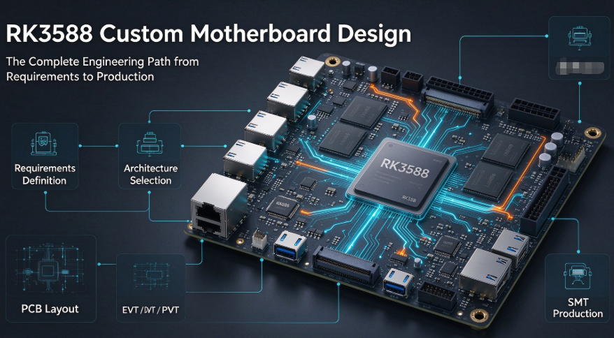
RK3588 custom motherboard design refers to the entire process of designing a board around the Rockchip RK3588 processor according to the specific interface, size, power consumption, and environmental requirements of a product. This process covers requirements definition, hardware design, software adaptation, verification and certification, and mass production. A typical workflow consists of eight stages:
- Requirements Definition and Feasibility Assessment (1–2 weeks)
- Solution Selection: System-on-Module (SoM) + Carrier Board, or Fully Custom Chip-Level Design (1 week)
- Schematic Design and Review (2–4 weeks)
- PCB Layout and High-Speed Signal Simulation (3–6 weeks)
- BSP / Driver / System Adaptation (in parallel, 4–8 weeks)
- Prototyping, Debugging, and Validation (3–5 weeks)
- Certification and Reliability Testing (4–12 weeks)
- Pilot Production and Mass Production (3–6 weeks)
Overall timeline: The SoM + carrier board solution typically takes 2–4 months to complete mass-production preparation, while a fully custom chip-level design typically takes 5–9 months. The actual timeline depends on requirement complexity, certification requirements, and team experience.
1. Why Is the RK3588 Suitable for Custom Motherboard Design?
The RK3588 is a flagship SoC developed by Rockchip using an 8nm process. It is designed for edge AI, multi-display systems, industrial control, and high-performance embedded applications. Its main specifications are as follows (refer to Rockchip’s official datasheet for specific details):
| Item | Main Specifications |
|---|---|
| CPU | 4× Cortex-A76 + 4× Cortex-A55, octa-core big.LITTLE architecture |
| GPU | Arm Mali-G610 MP4 |
| NPU | Approximately 6 TOPS computing power, supporting INT4/INT8/INT16/FP16 |
| Video | Up to 8K video decoding and 8K video encoding |
| Memory | Supports LPDDR4 / LPDDR4X / LPDDR5, with capacities of up to 32GB |
| Display Interfaces | HDMI 2.1, DP 1.4, eDP, MIPI DSI, etc., supporting multiple independent displays |
| High-Speed Interfaces | PCIe 3.0, PCIe 2.0, USB 3.1, SATA 3.0, dual Gigabit Ethernet (some interfaces share multiplexed functions) |
| Camera | Multiple MIPI CSI interfaces, supporting multiple camera inputs |
General-purpose development boards often cannot simultaneously meet requirements for size, interface combinations, power consumption, thermal management, and cost. This is where custom motherboard design delivers its value:
- Precise Interface Matching: Retain only the interfaces required by the product, eliminate redundant ones, and reduce BOM costs.
- Mechanical Adaptation: Customize the board shape according to the enclosure, cooling requirements, and mounting method.
- Controllable Reliability: Design wide-temperature operation, protection, power protection, and other features according to the application environment.
- Supply Chain Autonomy: Maintain control over key components to facilitate long-term supply and cost optimization.
- Software Integration: Deeply integrate the operating system, drivers, and product functions to improve stability.
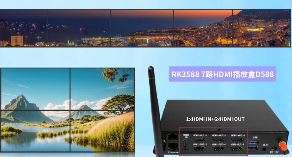
Typical applications: Edge AI boxes, multi-display video walls and digital signage, industrial tablets and HMIs, machine vision systems, intelligent cockpits and in-vehicle terminals, NVRs/video analytics gateways, robot controllers, medical imaging equipment, and more.
2. Step 1: Requirements Definition
Unclear requirements are the biggest cause of delays and rework in custom projects. Before starting the design, it is recommended to prepare a written Product Requirements Specification (PRS) that includes at least the following information.
2.1 Performance and Functional Requirements
- Target computing performance: CPU workload, NPU model scale (such as the number of YOLO streams and frame rate), and the number and resolution of video encoding and decoding streams.
- Memory and storage: RAM capacity and eMMC/UFS/NVMe/TF card configurations.
- Operating system: Android, Linux (Debian/Ubuntu/Buildroot/Yocto), or other systems.
2.2 Interface List
List the quantity and specifications of each interface individually, for example:
- Display: HDMI output/input, DP, eDP, MIPI DSI (number of lanes, resolution, and refresh rate)
- Networking: Gigabit/2.5G Ethernet, Wi-Fi 6/6E, Bluetooth, and 4G/5G modules
- Buses: UART, RS485, RS232, CAN/CAN-FD, I2C, SPI, and GPIO
- USB: Number of USB 3.0 / 2.0 ports and whether DP output is required through Type-C
- Expansion: PCIe slots, M.2, SATA, and Mini PCIe
- Cameras: Number of MIPI CSI interfaces and sensor models
- Audio: Line-in/line-out, microphone arrays, and power amplifiers
2.3 Environmental and Reliability Requirements
- Operating temperature: Commercial grade (0–70°C) or industrial grade (-40–85°C)
- Cooling method: Passive cooling, fans, or thermally conductive structural components
- Protection and interference resistance: ESD, EMC, surge protection, and waterproof/dustproof ratings
- Power supply: Input voltage range (e.g., DC 9–36V), power consumption budget, and power-loss protection
2.4 Commercial Requirements
- Target BOM cost and unit price for mass production
- Annual production volume and initial order quantity
- Product launch timeline
- Long-term supply period (e.g., 5–10 years)
- Required certifications (CE, FCC, CCC, RoHS, automotive-grade or medical certifications, etc.)
Practical recommendation: Divide requirements into three levels: Must / Should / Nice to Have. Optional features can be removed in the early stages to shorten the development cycle and added later through subsequent product revisions.
3. Step 2: SoM Solution vs. Fully Custom Chip-Level Design
This is the most critical architectural decision in RK3588 customization.
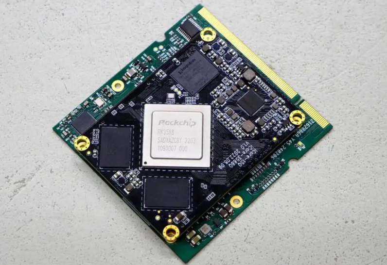
| Comparison Item | SoM + Custom Carrier Board | Fully Custom Chip-Level Design (All-in-One Motherboard) |
|---|---|---|
| Development Cycle | Short, approximately 2–4 months | Long, approximately 5–9 months |
| Initial Investment (NRE) | Low | Relatively high |
| Design Risk | Low, as the core section has already been validated | Relatively high, as DDR, power supply, and high-speed design must be completed independently |
| Unit Cost (High Volume) | Relatively high | Can be optimized, with significant advantages at high volumes |
| Size Flexibility | Limited by the dimensions of the SoM | Maximum flexibility, allowing the smallest possible form factor |
| Software Support | Suppliers usually provide a mature BSP | Adaptation must be developed independently or jointly |
| Suitable Applications | Small and medium production volumes, fast time to market, and validation stages | High annual production volumes, cost-sensitive applications, and compact structures |
Solution Selection Recommendations:
- For annual production volumes below approximately 5,000 units, or for first-time RK3588 product development, prioritize the SoM + custom carrier board solution to reduce risks.
- For high annual production volumes and extremely demanding cost and size requirements, adopt fully custom chip-level design.
- A hybrid approach: First use the SoM solution to validate the market and begin shipping products. Once sales stabilize, upgrade to a fully custom version.
4. Step 3: Key Considerations for Schematic Design
During the schematic design stage, strictly follow Rockchip’s official reference designs and hardware design guidelines, making modifications and extensions based on these references.
4.1 Power Tree Design
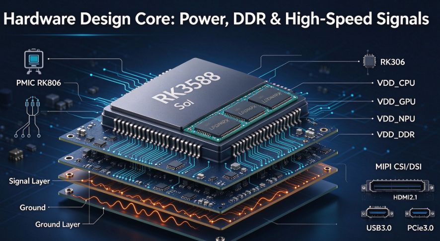
The RK3588 has stringent requirements for power sequencing and ripple. Official designs typically use a dedicated PMIC, such as the RK806 series. Key considerations include:
- Power-up/power-down sequencing: Strictly follow the timing requirements specified in the datasheet.
- Current headroom for each power rail: Reserve 20–30% current headroom for the CPU, GPU, NPU, and DDR under full load.
- Decoupling capacitors: Follow the quantities and capacitance values recommended in the official design. Plan the placement of capacitors beneath the BGA in advance.
- Input protection: Reverse-polarity, overvoltage, surge, and overcurrent protection.
4.2 DDR Design
- Prioritize memory chip models that have been validated by Rockchip, and avoid arbitrary substitutions.
- Confirm the topology, termination, and reference voltage requirements for LPDDR4/4X/5.
- Ensure that the memory capacity, number of memory chips, and operating frequency are consistent with the software memory configuration (DDR parameters).
4.3 Interfaces and Multiplexing
Some high-speed interfaces on the RK3588 have multiplexing relationships (for example, among PCIe, SATA, USB 3.0, and certain display interfaces). Multiplexing conflicts must be identified during the schematic design stage to avoid discovering after design completion that certain interfaces cannot be used simultaneously.
4.4 Boot and Debugging
- Reserve a UART debugging port, flashing/Maskrom buttons, and a USB flashing interface.
- Reserve test points for critical power rails and clock signals.
- Design a boot selection mechanism for eMMC and TF cards.
4.5 Schematic Review
At least two rounds of review are recommended: an internal cross-review and a review by the original chip manufacturer or an experienced third party. Key areas to check include power sequencing, multiplexing conflicts, interface voltage-level compatibility, and ESD protection.
5. Step 4: PCB Layout and High-Speed Signals
The RK3588 uses a high-density BGA package, making PCB layout relatively challenging. This is the stage where project risks are most concentrated.
5.1 Layer Stackup and Manufacturing Processes
- Layer count: Core boards and all-in-one motherboards commonly use 8–12 layers. Carrier boards alone can use 4–8 layers, depending on interface complexity.
- Manufacturing processes: BGA fan-out typically requires small via diameters and fine trace widths and spacing. Some designs use HDI technology (blind/buried vias, 1+N+1).
- Impedance control: 50Ω single-ended and 90Ω/100Ω differential, configured according to the specifications of each interface. Confirm the stackup with the PCB manufacturer.
5.2 Key Signal Routing Principles
| Signal Type | Key Requirements |
|---|---|
| DDR | Strict length and timing matching, grouped routing, complete reference planes, and placement according to official guidelines |
| PCIe / USB 3.0 | Strict differential-pair length matching, minimal vias, and avoidance of crossing plane splits |
| HDMI / DP / eDP | Continuous impedance, distance from noise sources, and proper ESD protection |
| MIPI CSI/DSI | Length matching within channel groups and consistent differential-pair routing |
| Ethernet | Maintain proper clearance and separation around the transformer area and ensure an appropriate distance between the PHY and the interface |
| Power | Use copper pours or wide traces for high-current paths to reduce voltage drops and ripple |
5.3 Thermal Design
The RK3588 can consume considerable power under full load, so the following aspects must be considered simultaneously:
- Coordinate large copper areas, thermal vias, thermal pads, and the mechanical design of heat sinks/fans.
- Determine the frequency-throttling strategy under high-temperature operating conditions through thermal simulation or actual measurements.
- For industrial wide-temperature products, evaluate the junction temperature under the most extreme environmental conditions in advance.
5.4 Signal Integrity and Power Integrity (SI/PI)
Simulation and validation are recommended for high-speed DDR and PCIe interfaces. When necessary, use oscilloscopes and network analyzers during prototyping to measure eye diagrams and reduce the likelihood of rework.
6. Step 5: Software and BSP Adaptation
Software development should begin alongside hardware design to shorten the overall project timeline.
- Bootloader and kernel: Adapt the device tree (DTS) based on Rockchip’s official SDK (Linux/Android).
- DDR parameters and initialization: Generate and debug DDR configurations according to the actual memory chip models.
- Driver adaptation: Display panels, touchscreens, camera sensors, Wi-Fi/4G modules, audio codecs, RTCs, sensors, and other components.
- NPU deployment: Use the RKNN toolchain to convert and deploy models, and evaluate inference performance.
- System customization and firmware: Customize the file system, boot process, OTA updates, and mass-production flashing solutions according to product requirements.
- Power management and stability: Adjust frequency and thermal management strategies, and conduct long-duration burn-in tests.
7. Step 6: Prototyping, Debugging, and Validation
7.1 Prototyping Stage
- For the first prototype run, 3–10 boards are recommended to cover different assembly variants and debugging requirements.
- Prioritize bringing up the minimum system: Power → Clock/Reset → DDR → Boot → Serial Console Output.
7.2 Functional Validation Checklist
- Voltage, ripple, and timing tests for all power rails
- DDR stress testing (such as long-duration memory tests)
- Functional and performance testing of all interfaces: USB, PCIe, networking, displays, cameras, and audio
- Full-load and temperature-rise testing for the CPU/GPU/NPU
- High- and low-temperature testing and long-duration stability testing
7.3 Design Iterations
Most RK3588 projects go through 1–2 board revisions. It is recommended to reserve jumpers, optional component footprints, and test points in the first design to improve debugging efficiency.
8. Step 7: Certification and Reliability Testing
Plan certifications in advance according to the target market and industry.
| Market/Industry | Common Certifications |
|---|---|
| China | CCC, SRRC (including wireless), CQC |
| European Union | CE (EMC, RED, LVD), RoHS, REACH |
| United States | FCC, UL |
| Industrial | Wide-temperature testing, vibration and shock testing, EMC immunity testing (surge, EFT/burst, ESD) |
| Automotive/Medical | Relevant industry standards, with longer certification cycles |
Note: Certification costs and timelines are often underestimated. It is recommended to conduct pre-compliance testing during the prototype stage and allow an additional 2–4 weeks for EMC rectification.
9. Step 8: Pilot Production and Mass Production
9.1 DFM / DFT Review
- DFM (Design for Manufacturability): Check component spacing, BGA pads, stencil apertures, panelization methods, process edges, and fiducial marks.
- DFT (Design for Testability): Design test points and plan ICT/FCT test fixtures and flashing solutions.
9.2 Small-Batch Pilot Production
- Typically 50–500 units, used to validate yield, process stability, and assembly procedures.
- Complete burn-in testing and reliability verification, such as drop and vibration testing, at the same time.
9.3 Supply Chain Preparation
- BOM optimization and alternative components: Prepare alternatives for critical components to prevent shortages from affecting delivery.
- Advance procurement of long-lead-time materials: Such as LPDDR memory chips, eMMC, and PMICs.
- PCBA processes: BGA placement and X-ray inspection, reflow soldering profile control, conformal coating, and other processes.
9.4 Mass Production Management
- Establish procedures for mass-production flashing, FCT testing, burn-in, and outgoing inspection.
- Establish version management and engineering change control (ECN) to ensure batch-to-batch consistency.
- Plan after-sales support and OTA update mechanisms.
10. Timeline and Cost References
The following figures represent common industry ranges and are provided for project planning purposes only. Actual timelines and costs depend on specific requirements and quotations.
| Stage | SoM + Carrier Board | Fully Custom Chip-Level Design |
|---|---|---|
| Requirements and Solution Planning | 1–2 weeks | 2–3 weeks |
| Schematic Design | 1–2 weeks | 3–4 weeks |
| PCB Layout | 2–3 weeks | 4–6 weeks |
| Prototyping and Debugging | 2–4 weeks | 4–6 weeks |
| BSP Adaptation | In parallel, 2–6 weeks | In parallel, 6–10 weeks |
| Certification and Pilot Production | 4–8 weeks | 6–12 weeks |
| Total | Approximately 2–4 months | Approximately 5–9 months |
Cost Components:
- One-time NRE costs: Hardware design, software adaptation, prototyping, test fixtures, and certification fees.
- BOM costs: Processor, memory, storage, power management chips, interface components, mechanical parts, and other components.
- Manufacturing costs: SMT assembly, testing, burn-in, and packaging.
- Hidden costs: Board revisions, component shortages, certification-related rectification, and project delays.
11. Common Design Pitfalls and How to Avoid Them
- Frequent requirement changes: Start PCB layout only after requirements have been frozen. Any subsequent changes should go through a formal review process.
- Interface multiplexing conflicts: Verify the multiplexing relationships among PCIe, USB 3.0, SATA, and display interfaces individually during the schematic design stage.
- Arbitrary DDR chip substitutions: Unvalidated memory models may cause instability. Always refer to the official compatibility list.
- Insufficient power supply headroom: Voltage drops and unexpected restarts may occur under full load. Reserve sufficient current and thermal headroom during design.
- Overlooking thermal management: The board may work normally in the laboratory but experience frequency throttling or system crashes in high-temperature environments.
- Addressing EMC issues too late: Discovering excessive emissions just before mass production can make corrective work costly.
- Starting software development too late: Beginning BSP adaptation only after hardware completion extends the overall project timeline.
- Supply chain risks: Critical components may become unavailable or reach end-of-life without an alternative component plan.
- Missing test points and flashing solutions: Efficient testing and firmware flashing may be impossible during mass production.
- Ignoring long-term supply: For products with long lifecycles, evaluate the supply availability period of the processor and critical components.
12. How to Choose an RK3588 Customization Partner
When evaluating design service providers or solution companies, consider the following criteria:
| Evaluation Dimension | Key Considerations |
|---|---|
| Project Experience | Whether the provider has RK3588 mass-production experience in similar industries |
| Technical Capabilities | Whether the team has comprehensive expertise in hardware, high-speed PCB layout, BSP development, and NPU deployment |
| One-Stop Services | Whether the provider can deliver design, prototyping, PCBA manufacturing, testing, and final delivery |
| Quality Management System | ISO 9001, traceability, and test coverage |
| Communication and Deliverables | Transparent milestones, complete documentation, and delivery of all source files |
| Intellectual Property | Clear ownership and confidentiality terms for schematics, PCB designs, and source code |
| After-Sales and Long-Term Support | Responsiveness to design revisions, long-term component supply, and software maintenance capabilities |
13. Frequently Asked Questions (FAQ)
Q1: How long does it take to develop an RK3588 custom motherboard?
Using an SoM + custom carrier board solution, it typically takes approximately 2–4 months to reach mass-production readiness. Fully custom chip-level design typically takes approximately 5–9 months. Certification requirements, requirement stability, and team experience can significantly affect the timeline.
Q2: How many PCB layers are required for an RK3588 custom motherboard?
Fully custom chip-level motherboards typically use 8–12 layers, with HDI technology potentially required for high-density designs. Carrier boards alone generally use 4–8 layers, depending on interface complexity.
Q3: How should I choose between an SoM solution and a fully custom design?
The SoM solution is recommended for lower annual production volumes, faster time-to-market requirements, or first-time RK3588 product development. Fully custom chip-level design is recommended for high production volumes and strict cost and size requirements. Another option is to validate the market using an SoM solution first and then upgrade to a fully custom design.
Q4: How much does RK3588 custom motherboard development cost?
Costs vary significantly depending on the solution type, interface complexity, software workload, and certification scope. It is recommended to provide a Product Requirements Specification and request an itemized quotation from the service provider covering hardware design, software adaptation, prototyping, certification, and test fixtures.
Q5: Can the RK3588 support multi-display output and AI inference?
Yes. The RK3588 supports multiple display output interfaces, including HDMI, DP, eDP, and MIPI DSI, as well as approximately 6 TOPS of NPU computing power. It is commonly used in multi-display systems, digital signage, and edge AI applications. The actual number of displays that can operate simultaneously and their supported resolutions depend on interface multiplexing and bandwidth limitations, which must be confirmed during the design stage.
Q6: Can an RK3588 custom motherboard support industrial wide-temperature operation?
Yes, but components that meet wide-temperature requirements must be selected, including memory, storage, and power management chips. The design must also be validated through high- and low-temperature testing. Wide-temperature solutions generally have higher BOM costs and longer validation cycles.
Q7: Who owns the schematics and source code after the design is completed?
Ownership depends on the contractual agreement. Before starting cooperation, clearly define the intellectual property ownership and deliverables for schematics, PCB designs, BSP source code, and documentation.
Conclusion
RK3588 custom motherboard design is a systems engineering process covering requirements, hardware, software, manufacturing, certification, and supply chain management. The keys to success are:
- Clearly document requirements at the beginning and freeze critical specifications.
- Select the SoM or fully custom design approach according to production volume and project risk.
- Develop hardware and software in parallel, with particular attention to power supply design, DDR, and high-speed signals during the schematic and PCB layout stages.
- Plan certification, testing, and mass-production processes in advance to avoid costly rework later.
If you are planning an RK3588-based product, start by preparing an interface list, power consumption budget, target cost, and product launch timeline. Then discuss the project with a team experienced in mass production. This approach can help you avoid many common pitfalls and make the development process more efficient.