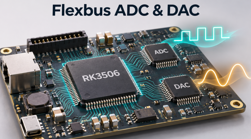
In industrial data acquisition, waveform generation, and embedded display projects, the interface between the processor and its peripherals can become a major design challenge. Software-driven GPIO toggling struggles to maintain consistent high-speed timing, while existing SPI or other dedicated controllers may not match the peripheral protocol.
The RK3506 Flexbus offers another option for these interface requirements. Its configurable hardware timing and data transfer mechanisms provide a way to connect certain external digital interfaces to the processor.
However, interface names alone do not determine compatibility. Before choosing Flexbus, developers need to verify data direction, clocking, control signals, available pins, and the driver implementation in the target board support package (BSP).
1. What Is RK3506 Flexbus?
Flexbus, short for Flexible Bus, is a configurable digital interface controller in the RK3506. It can adapt to certain standard or application-specific interface timings. Rockchip’s datasheet lists external ADCs, DACs, DVP cameras, and QSPI LCD panels as typical applications. [1]
The ADCs and DACs in these applications are external converters. Flexbus transfers digital sample data or digital output codes; it does not perform analog conversion. External circuitry remains responsible for the analog front end, reference voltage, filtering, and output drive.
A complete Flexbus implementation has three parts:
- Hardware connections: Pin multiplexing, logic levels, bit order, and clock direction.
- Controller and driver configuration: Data width, timing, transfer length, and interrupt handling.
- Application data handling: Buffer management, processing throughput, error recovery, and application protocols.
All three must work together. Enabling a device tree node alone does not establish reliable data acquisition or output.
2. Flexbus0 vs. Flexbus1: What Is the Difference?
The RK3506 Technical Reference Manual describes separate transmit and receive channels. The Flexbus0 data port supports input or output, while the Flexbus1 data port is used for input. The controller also supports built-in DMA and ping-pong operation using two addresses. [2]
| Resource | Data Direction and Typical Use | Development Considerations |
|---|---|---|
| Flexbus0 data port | Transmit or receive; typical uses include DAC output | Input, output, and combined modes must match the driver implementation |
| Flexbus1 data port | Receive; typical uses include ADC acquisition | Verify external clocking and sampling conditions |
| Controller DMA | Moves data between the interface and memory | Handle addresses, lengths, synchronization, and buffer ownership correctly |
| Ping-pong buffering capability | Provides a hardware basis for alternating between two buffers | Continuous operation still requires driver coordination and timely application processing |
Flexbus0 and Flexbus1 are not two identical, freely interchangeable general-purpose interfaces. To determine whether a particular transmit/receive combination can run simultaneously, check the controller mode, shared resources, and target BSP.
3. Which Applications Are Suitable for Flexbus?
Parallel ADC Data Acquisition
For an ADC with a parallel digital output, Flexbus can be evaluated as a receiving interface. Start by checking the output width, valid data window, sampling edge, and any additional signals such as BUSY, data-ready, or channel indicators.
An ADC is not automatically compatible with Flexbus simply because it is a converter. For devices with I²C or SPI interfaces, evaluate the corresponding dedicated controller first.
Parallel DACs and Waveform Generation
For a DAC with parallel inputs, Flexbus can be evaluated for transmitting digital code streams. Key considerations include the relationship between output data and the clock, the default output during startup, and the behavior when the data supply stops.
In actuator-control applications, define a safe output value for fault conditions at the system level. The output state after application software exits should be intentional and predictable.
DVP Camera Interfaces
DVP integration involves the pixel clock, line-valid signal, frame synchronization, and pixel data. In addition to electrical connections, verify support in the image capture driver, sensor control interface, and upper-level video framework.
Support for an image interface does not imply MIPI CSI-2 reception capability, nor does it establish a complete image-processing or video-encoding pipeline.
QSPI LCDs and Custom Interfaces
For a QSPI LCD, verify the number of active data lines and timing during the command, address, and data phases, along with chip-select hold behavior and readback requirements. For other custom peripherals, break the protocol into individual phases and determine whether the controller can implement each operation.
If the protocol requires complex dynamic handshaking, multiple independent clock domains, or strict real-time conditional behavior, also evaluate an FPGA, CPLD, or another interface solution.
4. Hardware Design: Define the Interface Before PCB Routing
Build a Peripheral Interface Requirements Table
Complete the following checks before schematic design to reduce the risk of discovering an incompatible interface during driver development.
| Item | Information to Confirm |
|---|---|
| Peripheral | Full part number, datasheet revision, and digital interface mode |
| Data direction | Input only, output only, or direction changes between phases |
| Data format | Width, bit order, signed or unsigned representation, and valid bit positions |
| Clock relationship | Clock source, operating frequency, sampling edge, and idle state |
| Control signals | Chip select, reset, enable, synchronization, and data-valid signals |
| Electrical requirements | I/O voltage, input thresholds, drive strength, and loading |
| Data continuity | Whether transfers can pause, sample loss is acceptable, and flow control is available |
| Software baseline | SDK version, driver mode, available examples, and application interface |
Verify Pins for the Exact Chip and Package
Do not determine pin locations from the RK3506 family name alone. Use the exact chip variant, package, and board schematic to check whether the required Flexbus signals are accessible and whether they share pins with Ethernet, display, or other peripherals.
When using a system-on-module (SoM), check the carrier-board connector pinout as well. A function supported by the chip may not be fully exposed by the module.
Confirm Logic-Level Compatibility
Check both the relevant RK3506 I/O power domain and the peripheral’s digital interface supply. If level translators are required, evaluate propagation delay, channel-to-channel skew, direction control, and power-up behavior in addition to voltage compatibility.
On a parallel bus, excessive differences in delay between data lines can reduce the receiver’s valid sampling window.
Route According to the Timing Budget
PCB layout should account for relative clock-to-data delay, continuous reference planes, return paths, and connector discontinuities. Keep clock traces away from strong interference sources such as switching power nodes.
Avoid applying a fixed length-matching tolerance or series resistor value without considering the operating frequency and timing requirements. Determine termination requirements and resistor values from driver characteristics, interconnect behavior, and measurements.
5. Linux Development Workflow: From BSP Review to the First Data Block
Step 1: Record the Hardware and Software Baseline
At a minimum, record the chip variant, board revision, SDK release, kernel commit, and device tree actually loaded by the system.
uname -a
cat /proc/device-tree/model
dmesg | less
Different vendors may provide different driver implementations for the same chip. Without version information, debugging results can be difficult to reproduce.
Step 2: Locate the Implementation in Your Source Tree
Run the following command from the kernel source root:
rg -n -i 'flexbus' drivers include Documentation arch/arm/boot/dtsLook for the controller driver, mode-specific drivers, Kconfig entries, device tree binding documentation, and examples for the target board. Directory layouts vary between SDKs, so adjust the search scope to your source tree.
Do not copy device tree nodes directly from the RK3576 or another platform. Even when function names match, register addresses, clocks, resets, pin groups, and supported modes may differ.
Step 3: Enable the Required Kernel Configuration
Use the current Kconfig definitions to verify that the controller driver, target mode driver, and required subsystems are enabled. After compilation, confirm that the driver is included in the image or modules deployed to the board.
ADC, DAC, camera, and display applications may use different upper-level interfaces through IIO, video, or display subsystems. Follow the interface exposed by the actual driver rather than assuming every Flexbus mode provides a common character device.
Step 4: Configure and Validate the Device Tree
Check the following:
- The controller and target function nodes are enabled.
- Pin groups match the board connections and have no multiplexing conflicts.
- Clock and reset resources are complete.
- Data direction, width, and timing properties are supported by the driver.
- Peripheral power, reset, and associated control interfaces are configured.
Device tree properties are not arbitrary parameter names. Each property should have a corresponding definition in the current binding documentation or implementation in the driver’s parsing code.
A generic DTS template without board-level validation can be misleading. Use the RK3506 configuration provided with your BSP as the starting point and verify each change against the hardware.
Step 5: Validate the Link with Low-Speed, Short Transfers
Begin with a clock below the target rate and short data blocks. If the peripheral provides test patterns or digital loopback, use those features first.
Useful test patterns include all zeros, all ones, alternating bits, incrementing counters, and walking-bit patterns. These help identify stuck levels, reversed bit order, data misalignment, and missing samples.
Use an oscilloscope to inspect voltage levels, edges, and overshoot, and a logic analyzer to check protocol sequencing. Receiving data in software does not, by itself, demonstrate adequate electrical timing margin.
6. DMA and Continuous Acquisition: Key Considerations
Distinguish Between Three Data Widths
The peripheral’s valid data width, the bus transfer width, and the memory storage width may differ. For example, a 12-bit sample might occupy a 16-bit storage unit, but the actual arrangement must be confirmed from the driver implementation and peripheral format.
Calculate bandwidth using the actual number of stored bytes. When parsing data, account for valid bit positions, sign extension, and byte order.
Manage Buffers Through the DMA API
Kernel drivers should use the Linux DMA API to manage DMA addresses and cache coherency. A normal userspace pointer is not a DMA address, and physical addresses should not be inferred without a valid mapping.
Define when the CPU or DMA engine owns each buffer and when that buffer may be read, modified, or reused.
Check Length Units and End-of-Transfer Handling
A register’s transfer length may represent bytes, data units, or another quantity. Check both the technical manual and current driver before configuring it.
Test transfers that do not fill an entire block. Verify the valid data length, any padding, and application parsing so that padding is not mistaken for samples.
Ping-Pong Buffering Does Not Guarantee Lossless Capture
Double buffering allows hardware transfers and CPU processing to overlap. If the application cannot keep up over time, buffers may still be overwritten or overflow.
For continuous acquisition, record block sequence numbers, valid sample counts, error flags, and timing information. For sources without flow control, define what happens when no free buffer remains.
7. How to Estimate Flexbus Bandwidth and Buffer Size
Start with the application’s data volume, then determine whether the interface and system can sustain it.
Memory data rate = Samples per second × Stored bytes per sample.
For example, assume an application requires 10 MS/s and stores each sample in 16 bits:
10,000,000 × 2 = 20,000,000 B/s, or approximately 20 MB/sBuffering 100 ms of data would require approximately 2 MB in theory. This is a calculation example, not a verified RK3506 performance result. Additional capacity is needed for scheduling jitter, copying, algorithm processing, and storage stalls.
For a clocked parallel interface, estimate theoretical data-line throughput as follows:
Theoretical throughput = Interface clock frequency
                        × Valid transfers per clock cycle
                        × Data width in bits ÷ 8
Theoretical throughput is not the same as sustained application throughput. The proportion of valid data, DDR contention, interrupt frequency, cache management, and application processing can all affect the result.
Measure interface reception, memory movement, application reads, and final processing separately to identify the actual bottleneck.
8. Common RK3506 Flexbus Problems and Troubleshooting
| Symptom | Check First | Recommended Action |
|---|---|---|
| No clock output | Clock direction, clock gating, pin multiplexing, and transfer trigger conditions | Confirm which endpoint supplies the clock in the selected mode and measure during transfer startup |
| Data is all zeros or all ones | Peripheral operation, wiring, logic levels, and enable state | Confirm that valid transitions exist at the peripheral output |
| Clearly incorrect values | Bit order, byte order, valid bit positions, and sign extension | Apply known test codes and verify each bit |
| Intermittent misalignment or unexpected code changes | Sampling edge, timing margin, and signal integrity | Reduce the rate and examine the clock-to-data relationship |
| Transfer timeout | Missing external clock, unmet data conditions, interrupt problems, or DMA faults | Correlate waveforms, logs, interrupt counts, and driver state |
| Short transfers work but continuous operation fails | Buffer reuse, insufficient application throughput, and memory contention | Record block sequence numbers, queue depth, and error counts |
| Samples are lost when networking or display tasks start | System bandwidth or scheduling pressure | Add workloads individually and measure when the problem appears |
| DVP images show displaced lines or incorrect colors | Synchronization polarity, data mapping, and pixel ordering | Use the sensor’s test pattern and verify one setting at a time |
Change one key variable at a time and retain before-and-after logs and waveforms. Changing frequency, pins, and buffer settings together makes the root cause difficult to isolate.
9. Validation Checklist: From Prototype to Production
A prototype that receives one data block is only the starting point. Product validation should cover:
- Functional coverage: Normal startup, stop, repeated startup, and different transfer lengths.
- Data integrity: Bit order, valid length, block order, and loss detection.
- System stress: Concurrent display, networking, storage, and algorithm workloads.
- Fault recovery: Peripheral resets, interrupted clocks, transfer timeouts, and application termination.
- Environmental operation: Testing under the product’s specified temperature, power, and cable conditions.
- Version traceability: Schematics, BOM, device tree, kernel commit, and test program versions.
Write acceptance criteria as measurable conditions, such as a defined data rate, operating duration, and maximum permitted error count. A general statement that the system “works normally” is insufficient for production approval.
10. Frequently Asked Questions
How Does RK3506 Flexbus Differ from Standard GPIO?
Standard GPIO provides pin-level input and output control. Flexbus provides dedicated timing and data transfer mechanisms. For higher data rates or continuous streams, evaluate hardware interface support rather than relying on repeated software-driven GPIO toggling as a stable high-speed bus.
Can Flexbus Replace an FPGA?
Flexbus may be suitable for some simple interface adaptations. Complex logic, multiple parallel processing paths, and strict real-time control require a separate assessment. Protocol complexity, latency, and resource requirements should determine whether an FPGA is needed.
Are Flexbus and DSMC the Same Interface?
No. Rockchip lists Flexbus and DSMC as separate peripheral resources. [3] Distinguish streaming-interface requirements from external memory or local-bus access requirements, then verify the appropriate controller and driver.
Can I Reuse Flexbus Examples from Other Rockchip Platforms?
Their development approach can be useful, but porting requires checking RK3506 resource definitions, driver versions, and board connections. Device tree addresses, clocks, resets, and pin configurations must be reviewed rather than copied unchanged.
What Is the Maximum Flexbus Transfer Rate?
The usable rate depends on the exact chip documentation, operating mode, peripheral timing, PCB implementation, and driver validation. Evaluate sustained throughput and error rate under the intended operating conditions rather than promising sampling performance based on a clock frequency alone.
Conclusion
Successful RK3506 Flexbus development connects the peripheral protocol, electrical timing, driver configuration, and memory data handling into a verifiable data path. Confirming interface compatibility first, followed by low-speed tests, DMA validation, and system stress testing, can reduce later PCB revisions and debugging effort.
If you are developing an RK3506-based data acquisition device, industrial controller, or custom display product, contact the LST engineering team to discuss interface requirements, hardware and PCB design, Linux driver adaptation, and PCBA manufacturing and testing. Sharing the peripheral part number, target data rate, system version, and existing schematic helps accelerate a feasibility review.